
 Recently Expanded in Speeds is the CeleronTM.
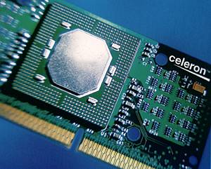
An inexpensive path to Pentium II architecture, the Celeron is basically a cut - down Pentium II processor. All models (333 to 433) use a smaller 128kB cache to reduce the price. (The first two models released in the Celeron range, the 266 and 300 had no cache - these have now been superseded)
The Celeron is supplied either in SEPP (Single Edge Processor Package) or PPGA (Plastic Pin Grid Array - commonly referred to as 'Socket 370')
The Celeron SEPP is completely compatible with standard 242CSC except that the processor cover plate of the Pentium II SECC package (required on the Pentium II because of greater cooling requirements) is omitted. A slightly different processor retention bracket is required for the SEPP compared to SECC.
The PPGA arrangement is similar to the old 'socket 7' mounting standard, but includes and additional row of pins. Unfortunately this means that 'Socket 7' motherboards WILL NOT support the Celeron processor, however an adapter plate is available to install PPGA Celerons on motherboards using the 242CSC system.
The Celeron processor is fully compatible with an entire library of PC software based on operating systems such as MS-DOS®, Windows® 3.1, Windows for Workgroups® 3.11, Windows® 98, Windows® 95, OS/2®, UnixWare®, SCO UNIX®, Windows® NT, OPENSTEP®, and Sun Solaris®.
Some of the Celeron features in detail:
- Dynamic Execution Technology:
Dynamic execution incorporates the concepts of out of order and speculative execution. The Celeron processor's implementation of these concepts removes the constraint of linear instruction sequencing between the traditional fetch and execute phases of instruction execution. Up to 3 instructions can be decoded per clock cycle. These decoded instructions are put into a buffer, which can hold up to 40 instructions. Instructions are executed from this buffer when their operands are available (versus instruction order). Up to 4 instructions can be executed per clock cycle.
- Superpipelining:
The pipeline of the P6 architecture consists of approximately 12 stages versus 5 for the Pentium processor and 6 for the Pentium processor with MMX technology. This enables the Celeron processor to achieve about a 50% higher frequency than the Pentium processor on the same manufacturing technology. The sophisticated, two-level, adaptive-training, branch prediction mechanism of the P6 microarchitecture is the key to maintaining the efficiency of the Intel Celeron processor's superpipelined microarchitecture.
- High Performance Intel MMX Technology:
Intel's MMX technology is a major enhancement to the Intel Architecture that enables PCs to provide richer multimedia and communications capabilities. This technology introduces 57 instructions oriented to highly parallel operations with multimedia and communications data types. These instructions use a technique known as SIMD (Single Instruction, Multiple Data) to deliver better performance for multimedia and communications computation. Intel processors that include MMX technology are fully compatible with previous generations of the Intel Architecture and the installed base of software. The Celeron processor, like the Pentium II processor, can execute 2 Intel MMX instructions simultaneously.
- Write Combining:
The Write Combining technology of the P6 architecture can be used to achieve very high graphics I/O performance. This feature combines multiple writes to a region of memory (for example, a video controller's frame buffer) declared as WC type into a single burst write operation. This is well suited for the bus, which is optimised for burst transfers. These writes are further combined by the chipset, leading to high throughput for graphics I/O. This further enhances multimedia performance and enables more realistic full motion video and fast, realistic graphics performance.
- Caches:
The Celeron processor has 32k of non-blocking L1 cache, which is divided into a 16k instruction cache and a 16k data cache. Each of these caches runs at the processor frequency and provides fast access to heavily used data. The 433, 400, 366, and 333MHz Celeron processors have a 128k full-speed L2 cache that is unified for code and data, and is non-blocking. A dedicated 64-bit bus facilitates higher data transfer rates between the processor and the L2 cache. A Floating-Point pipeline supports the 32-bit and 64-bit IEEE® 754 formats as well as the 80-bit format. The FPU is object code-compatible with the Pentium and i486 processor FPUs.
- Testing and Performance Monitoring Features:
Built In Self Test (BIST) provides single stuck-at fault coverage of the microcode and large PLAs, as well as testing of the instruction cache, data cache, Translation Lookaside Buffers (TLBs) and ROMs. IEEE® 1149.1 Standard Test Access Port and Boundary Scan Architecture mechanism allows testing of the Celeron processor through a standard interface. Internal performance counters can be used for performance monitoring and event counting.
 Back to Intel Processors Information
All promotional photographs and advertising material, corporate names and logos, product names, trade names, trademarks and registered trademarks are the property of their respective owners, and are acknowledged as such. Whilst every care is taken in the preparation of the information presented in these pages, ZCM Services can take no responsibility for errors or omissions.
Please report any problems encountered with these web pages to info@zcm.com.au
Copyright ©1997 ZCM Services, Australia. Last updated on May 10, 1999.