 The current workhorse in the Intel line is the Pentium IITM.
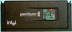
The Pentium II processor family offers significant improvements in performance and capabilities over it's predecessors.
At the physical level, the most obvious change is the abandonment of the old 'Socket 7' mounting system, in favour of the new '242 Contact Slot Connector' standard - commonly abbreviated to 242CSC. (Formerly referred to as 'Slot 1') The Pentium II is supplied in SECC (Single Edge Contact Cartridge) which mates with 242CSC. The 242CSC system greatly improves mounting rigidity, enhances processor cooling and requires a smaller mounting area. Unfortunately, this means that current 'Socket 7' motherboards cannot be upgraded to take advantage of these new processors.
At an electronic level, the level 2 cache which used to be external on the motherboard on 'Socket 7' implementations, and ran at external bus speed (usually 66MHz), is now tightly integrated within the 242CSC package and runs at half processor core speed. The 512kB cache tightly integrated in this manner provides significant speed improvements.
To obtain the benefit of the full capabilities of the Pentium II, Intel has developed the 440LX and 440BX support chipsets (other enhancements are in the pipeline). This allows peripherals like video cards access to the high speed data paths of the processor. (at 133MHz for example using the new AGP standard)
Nearly all motherboard designs incorporating these new chipsets and 242CSC will be the new ATX formfit standard, but most manufacturers are intending to offer at least some suitable AT formfit motherboards for the upgrade market.
The Pentium III processor is fully compatible with an entire library of PC software based on operating systems such as MS-DOS®, Windows® 3.1, Windows for Workgroups® 3.11, Windows® 98, Windows® 95, OS/2®, UnixWare®, SCO UNIX®, Windows® NT, OPENSTEP®, and Sun Solaris®.
Some of the new features in detail:
- Dynamic Execution Technology:
Dynamic execution incorporates the concepts of out-of-order and speculative execution. The Pentium II processor's implementation of these concepts removes the constraint of linear instruction sequencing between the traditional fetch and execute phases of instruction execution. Up to 3 instructions can be decoded per clock cycle. These decoded instructions are put into a buffer, which can hold up to 40 instructions. Instructions are executed from this buffer when their operands are available (versus instruction order). Up to 4 instructions can be executed per clock cycle.
- Superpipelining:
The pipeline of the P6 processor family consists of approximately 12 stages, versus 5 for the Pentium processor and 6 for the Pentium processor with MMX technology. This enables the Pentium II processor to achieve about a 50% higher frequency than the Pentium processor on the same manufacturing technology. The sophisticated, two-level, adaptive-training, branch prediction mechanism of the Pentium II processor is key to maintaining the efficiency of the superpipelined microarchitecture.
- Dual Independent Bus (DIB) Architecture:
This architecture consists of two distinct buses emanating from the Pentium II processor:
The L2 cache bus. The L2 cache bus speed scales with processor frequency. For the Pentium II processor at 266 MHz, the L2 cache bus operates at 133 MHz, which is twice the speed of Pentium processor systems.
The system bus (used for memory and I/O requests). The system bus for both processors runs at 66 MHz.
The net result is that the Pentium II processor at 266 MHz has about 3 times the peak bus bandwidth of the highest speed Pentium processor system, which has but one bus running at a peak of 66 MHz. Also, since speed of L2 cache accesses is one of the more important system factors in determining overall performance, system performance will scale well with higher processor frequencies.
Unlike the Pentium processor's system bus, the Pentium II processor's system bus supports up to 8 outstanding bus requests (4 per processor). This allows more parallelism between processors and I/O, as well as supporting smooth performance scaling to a 2 processor system. The GTL+ electrical signalling of the system bus facilitates the migration of this bus to higher frequencies as higher performance DRAM technologies come to market.
- High Performance Intel MMX Technology:
Intel's MMX media enhancement technology is a major extension of the Intel Architecture that makes PCs into richer multimedia and communications platforms. This technology introduces 57 instructions oriented to highly parallel operations with multimedia and communications data types. These instructions use a technique known as SIMD (Single Instruction, Multiple Data) to deliver better performance for multimedia and communications computation. Intel processors that provide MMX technology support are fully compatible with previous generations of the Intel Architecture and the installed base of software. To further improve performance, the Pentium II processor, like the Pentium processor with MMX technology, can execute 2 Intel MMX instructions at a time.
- Write Combining:
The Write Combining technology of the P6 architecture can be used to achieve very high graphics I/O performance. This feature combines multiple writes to a region of memory (for example, a video controller's frame buffer) declared as WC type into a single-burst write operation. This is well suited for the bus, which is optimised for burst transfers. The combining also leads to burst writes of cache line sizes. These writes are further combined by the chipset, leading to high throughput for graphics I/O. The result is enhanced multimedia performance, more realistic full-motion video, and realistic, fast graphics performance.
- Caches:
The Pentium II processor has 32 kB of non-blocking L1 cache, which is divided into a 16K instruction cache and a 16K data cache. Each of these caches runs at the processor frequency and provides fast access to heavily used data. The Pentium II processor has a 512k L2 cache which is unified for code and data, and is non-blocking. There is a dedicated 64-bit bus to facilitate higher data transfer rates between the processor and the L2 cache. The floating-point pipeline supports the 32-bit and 64-bit IEEE® 754 formats as well as the 80-bit format. The FPU is object code-compatible with the Pentium and i486 processor FPUs. The GTL+ bus provides glueless support for two processors, giving a cost-effective SMP solution. This can be used to significantly enhance OS and application performance in multithreaded or multitasking environments or for functional redundancy checking.
- Testing and Performance Monitoring Features:
Built In Self Test (BIST) provides single stuck-at fault coverage of the microcode and large PLAs, as well as testing of the instruction cache, data cache, Translation Lookaside Buffers (TLBs), and ROMs. IEEE® 1149.1 Standard Test Access Port and Boundary Scan Architecture mechanism allows testing of the Pentium II processor through a standard interface. Internal performance counters can be used for performance monitoring and event counting.
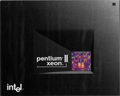

Pentium II XEONTM.
Specifically optimised for high end servers, the cache is increased in size to either 1MB or 2MB (depending on the model) and operates at FULL core processor speed. These changes make this the processor of choice in this demanding application.
 Back to Intel Processors Information
All promotional photographs and advertising material, corporate names and logos, product names, trade names, trademarks and registered trademarks are the property of their respective owners, and are acknowledged as such. Whilst every care is taken in the preparation of the information presented in these pages, ZCM Services can take no responsibility for errors or omissions.
Please report any problems encountered with these web pages to info@zcm.com.au
Copyright ©1997 ZCM Services, Australia. Last updated on May 7, 1999.